



Advanced Packaging Technologies Powering the AI Chip Race
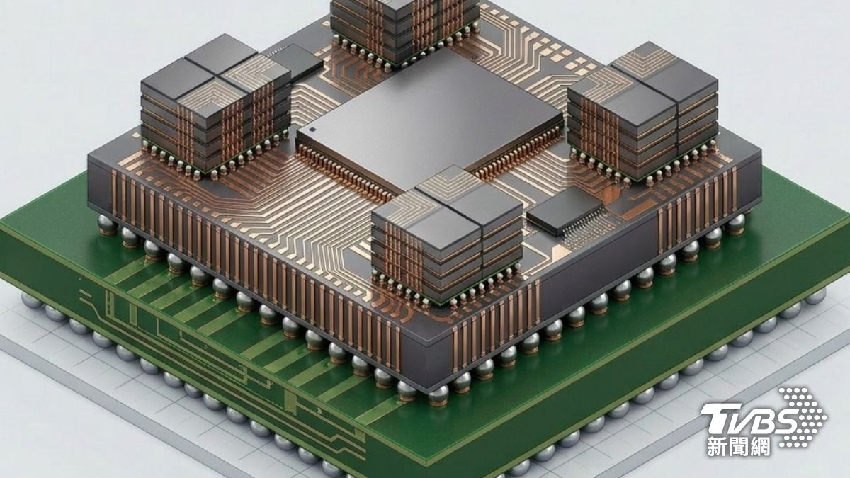
For decades, making chips faster meant shrinking transistors. That approach is hitting physical and economic limits. The semiconductor industry has found a powerful alternative: instead of building one giant chip, engineers now place several smaller chips side by side or stack them vertically inside a single package, connecting them with ultra-fast internal wiring. This is advanced packaging, and it has become the most critical bottleneck in the global AI supply chain.
Modern AI processors must move enormous volumes of data between computing cores and memory at speeds traditional designs cannot deliver. When a processor and its memory sit on separate packages connected through a circuit board, the physical distance creates a bandwidth wall. Advanced packaging eliminates that wall by bringing chips and memory together inside a tightly integrated unit.
Nvidia alone is consuming more than half of TSMC's 2026 advanced packaging output. TSMC says demand is growing at an 80% compound annual rate, and equipment suppliers can fill only about half of incoming orders. That scarcity has turned advanced packaging into a strategic battleground. Here are the six technologies that matter most.
CoWoS stands for Chip-on-Wafer-on-Substrate and is TSMC's flagship platform, found inside nearly every leading AI accelerator today. TSMC places processor chips and high-bandwidth memory stacks side by side on a thin silicon base called an interposer, which contains thousands of tiny vertical connections that create an ultra-dense data highway between them. The assembly is then mounted on a substrate that connects to the rest of the system.
CoWoS comes in two main variants. CoWoS-S uses a single silicon interposer and is the workhorse of current AI packaging. CoWoS-L uses a local silicon interconnect for even larger packages, enabling designs like Nvidia's Blackwell that link two processor chips too large to manufacture as one. TSMC controls more than 90% of the global CoWoS market and is expanding monthly capacity from roughly 80,000 wafers at the end of 2025 to 130,000 by late 2026.
PiFO stands for Pillar Integration Fan-Out. Developed by Taiwan's Powertech Technology over more than a decade, PiFO uses a glass substrate with copper pillar interconnects instead of a silicon interposer. Glass offers two advantages: it dissipates heat more effectively and is significantly cheaper to manufacture. Powertech claims PiFO matches TSMC's CoWoS-L at roughly 30% lower cost. Multiple US AI chip designers have locked in orders through 2027, and Powertech is investing NT$44.3 billion (US$1.4 billion) over three years to scale production. Full customer qualification is expected by the end of 2026.
Intel has developed two complementary platforms. EMIB, or Embedded Multi-die Interconnect Bridge, is a 2.5D technology that embeds small silicon bridges directly into the package substrate to connect neighboring chips. Think of each bridge as a short, high-speed tunnel linking two adjacent chips without a full-size silicon interposer underneath. This makes EMIB more cost-effective than CoWoS for certain designs while still delivering the bandwidth AI workloads demand. Its latest evolution, EMIB-T, adds through-silicon vias to support next-generation memory including HBM4.
Foveros is Intel's 3D stacking technology. Instead of placing chips side by side, Foveros bonds one chip directly on top of another using tiny copper connections, shrinking the footprint and shortening signal distances. When combined in a single package, the result is a 3.5D solution: chips stacked vertically with Foveros and connected horizontally with EMIB bridges. Intel's Penang, Malaysia packaging complex begins operations in 2026, and the company has outsourced EMIB production to Amkor in Songdo, South Korea, with additional capacity planned in Arizona.
FOCoS stands for Fan-Out Chip-on-Substrate. Developed by ASE, the world's largest outsourced packaging firm, FOCoS uses a fan-out redistribution layer to connect multiple chips on a substrate without a silicon interposer, reducing material cost while achieving the integration density that high-performance chips require. AMD and Broadcom are among early adopters, with volume production scheduled at ASE's Kaohsiung facility in the second half of 2026.
CoWoP stands for Chip-on-Wafer-on-PCB. Developed jointly by ASE's subsidiary SPIL and Nvidia, CoWoP eliminates the organic substrate layer entirely, mounting the chip-and-interposer assembly directly onto a printed circuit board. Removing the substrate reduces cost, shortens the signal path, and enables larger package sizes. Nvidia has designated CoWoP as a strategic long-term collaboration, though the technology remains in test verification with no confirmed mass production date.
As AI models grow larger and more power-hungry, the physical packaging around the chip has become just as important as the transistors inside it. No single company can meet global demand alone. TSMC's CoWoS dominates today, but the rapid development of PiFO, EMIB, Foveros, FOCoS, and CoWoP reflects an industry that recognizes advanced packaging as the defining competitive arena of the AI era. The companies that solve this challenge at scale will determine how fast the next generation of AI infrastructure can be built.