
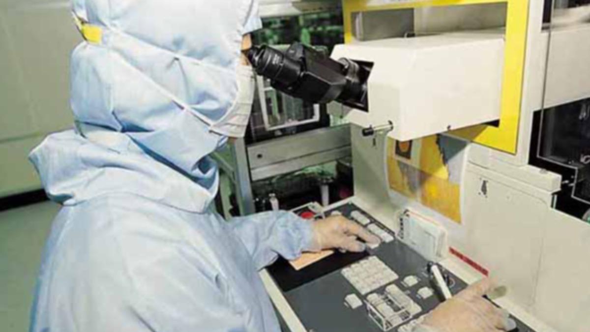
TSMC used its 2026 Technology Symposium in Hsinchu on May 14 to tell two stories. The first was about steel and concrete. The second was about light.
Vice president Bor-Zen Tien told the audience that TSMC now has 18 new 12-inch fabs and advanced packaging plants that are either under construction or have recently broken ground, including five dedicated to advanced packaging. The pace of the buildout in 2025 and 2026 is running at twice the average of the previous seven years, when the company opened roughly four fabs annually.
The geography is now genuinely global. The first Arizona fab entered 4nm mass production in 2024, and a second is scheduled for 3nm in the second half of 2027, with a third under construction and a fourth in planning alongside the first US advanced packaging plant. Construction on the second Kumamoto fab in Japan started in 2025. A new German fab will focus on automotive and industrial chips at 12 to 28nm. In Taiwan, 12 facilities are currently being built, including Hsinchu Fab 20 and Kaohsiung Fab 22 for the N2 generation, and Taichung Fab 25, due for mass production in 2028.
The most striking number was for CoWoS, the advanced packaging technology that stitches GPU dies to high-bandwidth memory in a single module. TSMC said CoWoS capacity will grow at a compound annual rate above 80 percent over the next several years. Second-generation SoIC, the more advanced 3D chip-stacking variant, has had its development time cut by roughly 75 percent.
The forum's most attention-grabbing announcement came from co-chief operating officer Kevin Zhang, who predicted that the global semiconductor market will reach US$1.5 trillion by 2030, with AI and high-performance computing accounting for roughly 55 percent and smartphones around 20 percent. The shift from training large AI models to running them for end users, or inference, will be the bigger growth driver, and it will reward designs that integrate logic, memory, and now optics in a single package.
That last word matters. Zhang told the audience to remember the acronym COUPE, which stands for Compact Universal Optical Communication Engine. It is TSMC's bet on co-packaged optics, an approach that replaces the electrical wiring between a chip and the rest of the system with light. COUPE-on-substrate is scheduled to enter production in 2026 and is projected to double power efficiency and cut latency by 90 percent compared with today's pluggable optical modules.
The headline numbers, 18 fabs under construction and CoWoS capacity growing above 80 percent a year, show a company racing to expand global AI chip manufacturing capacity to meet surging demand. The COUPE pitch describe the same firm quietly establishing the next physical standard for how AI systems communicate. These are not two separate stories, but one. TSMC is no longer merely scaling up AI chip production. It is defining the physics of artificial intelligence itself.