
The artificial intelligence revolution runs on silicon, but not just any silicon. The processors driving today’s most advanced AI systems demand a level of integration and performance that pushes semiconductor engineering to its limits. At the center of this challenge sits CoWoS (Chip-on-Wafer-on-Substrate), an advanced packaging technology developed by TSMC that has quietly become the essential foundation of AI infrastructure worldwide.
For decades, the semiconductor industry relied on shrinking transistors to deliver faster, more powerful chips. That approach is hitting physical and economic walls. As traditional scaling becomes more difficult, advanced packaging has emerged as the new frontier for performance gains. CoWoS represents this shift. Rather than simply making transistors smaller, it rethinks how multiple chips work together inside a single package, effectively extending Moore’s Law at the system level.
Modern AI workloads are extraordinarily data-hungry. Training large language models and running inference on complex neural networks requires processors to shuttle vast amounts of data between computing cores and memory at speeds that traditional chip designs simply cannot deliver. When a processor and its memory sit on separate packages connected through a circuit board, that physical distance creates a bandwidth bottleneck.
CoWoS eliminates this bottleneck through a three-layer architecture. The name describes the structure: chips are mounted on a silicon wafer (the interposer), which is then mounted on a substrate that connects to the rest of the system. The silicon interposer is the critical innovation. This thin slice of silicon sits between the active chips and the package substrate, providing an ultra-dense network of connections through thousands of tiny pathways called through-silicon vias. By placing processor dies and high-bandwidth memory stacks side by side on this interposer, CoWoS creates what amounts to a miniature data highway within the package itself.
Nearly every leading AI accelerator relies on CoWoS. Nvidia’s Blackwell GPUs use a variant called CoWoS-L (Local Silicon Interconnect) to connect two massive processor dies that would be impossible to manufacture as a single chip. AMD’s Instinct MI350 accelerators use CoWoS-S for similar reasons. The technology gives chip designers remarkable flexibility, allowing them to combine various processors and memory chiplets in a single package and tune configurations for specific workloads without redesigning entire chips from scratch.
The upcoming generation pushes boundaries even further. Nvidia’s Rubin architecture, entering trial production in early 2026, will use a 3nm process with a massive 4x reticle size interposer capable of integrating up to twelve stacks of next-generation HBM4 memory. TSMC is also developing CoWoS variants that combine with its SoIC (System on Integrated Chips) 3D stacking technology, enabling shorter vertical interconnects that reduce power consumption while increasing bandwidth.
TSMC controls more than 90% of the global CoWoS market, and competitors like Intel and Samsung trail years behind. This dominance has made CoWoS capacity one of the most critical chokepoints in the global semiconductor supply chain, particularly as AI demand has surged.
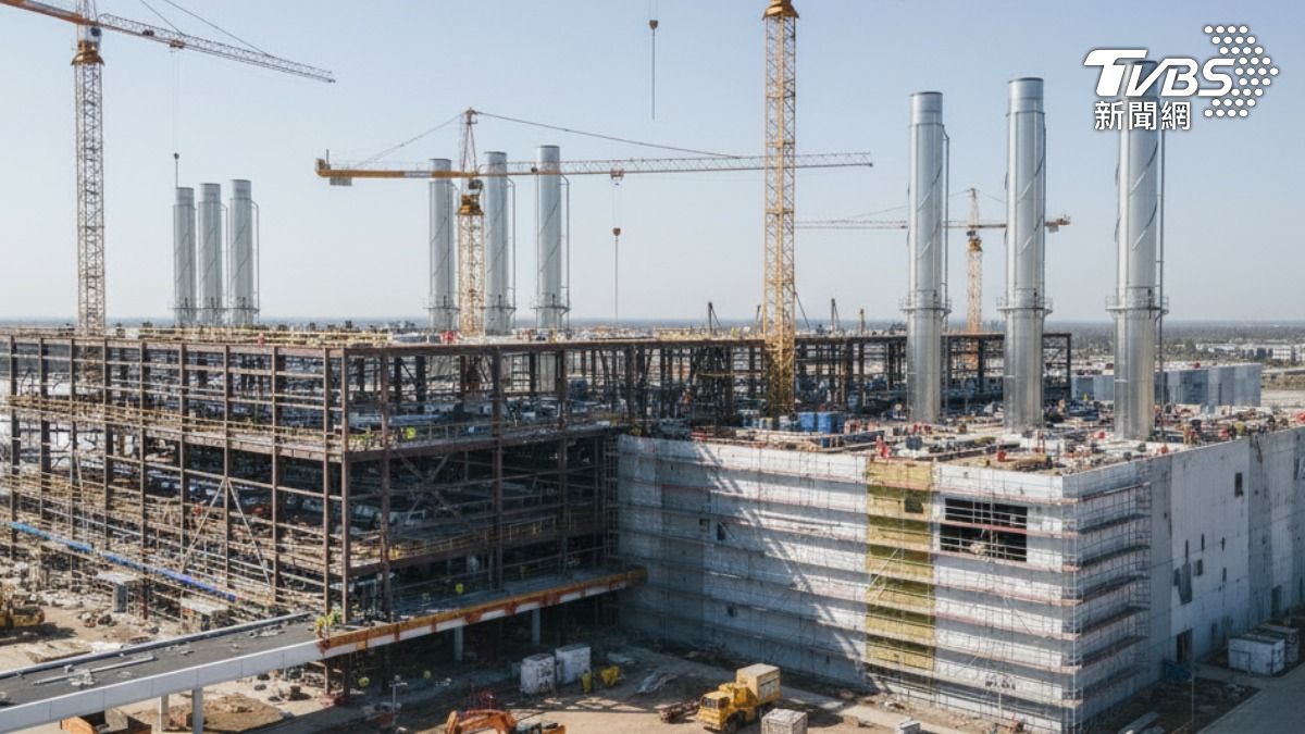
The numbers tell the story. TSMC’s monthly CoWoS output stood at roughly 75,000 to 80,000 wafers at the end of 2025. By late 2026, the company aims to reach 130,000 wafers per month, nearly quadrupling output from late 2024 levels. TSMC now allocates over 10% of its annual capital expenditure to packaging and testing, with its 2026 capex guidance of US$52 to $56 billion reflecting strong confidence in sustained demand. The company’s Chiayi AP7 complex is set to become the world’s largest advanced packaging hub, with multiple phases coming online through 2027.
While TSMC leads, the story extends well beyond a single company. Taiwan’s outsourced semiconductor assembly and test (OSAT) industry represents approximately US$21 billion in annual revenue and controls 48% of the global market. As demand outstrips even TSMC’s expanding capacity, these companies have become increasingly critical.
ASE Technology Holding, the world’s largest OSAT firm with US$20.78 billion in 2025 revenue, handles an estimated 40 to 50% of TSMC’s outsourced CoWoS packaging and is developing CoWoP (Chip-on-Wafer-on-PCB), a next-generation approach that could eventually eliminate substrates altogether. Powertech Technology’s proprietary PiFO (Pillar Integration Fan-Out) technology uses glass substrates that the company claims provide better heat dissipation at approximately 30% lower production costs.
The road ahead points toward even more ambitious integration. TSMC is developing CoPoS (Chip-on-Panel-on-Substrate), which uses rectangular 310mm panels instead of round wafers. This shift alone increases area utilization from roughly 57% to over 87%, reducing waste and manufacturing costs. Nvidia has reportedly selected CoPoS as foundational technology for future architectures beyond Rubin.
Equipment suppliers currently fulfill only about half of incoming orders from TSMC and its packaging partners, a bottleneck that underscores just how far demand has outpaced supply. That imbalance is unlikely to ease anytime soon. What began as an advanced packaging technique has become essential infrastructure, and the industry is still racing to build enough of it. By enabling the integration of multiple cutting-edge chiplets and memory modules into high-performance packages, CoWoS has set new standards for what AI processors can achieve. As workloads grow in complexity and scale, this technology and its successors will remain the foundation on which the next generation of computing is built.