



Lam Research: Panel-level approach key to scaling AI chips
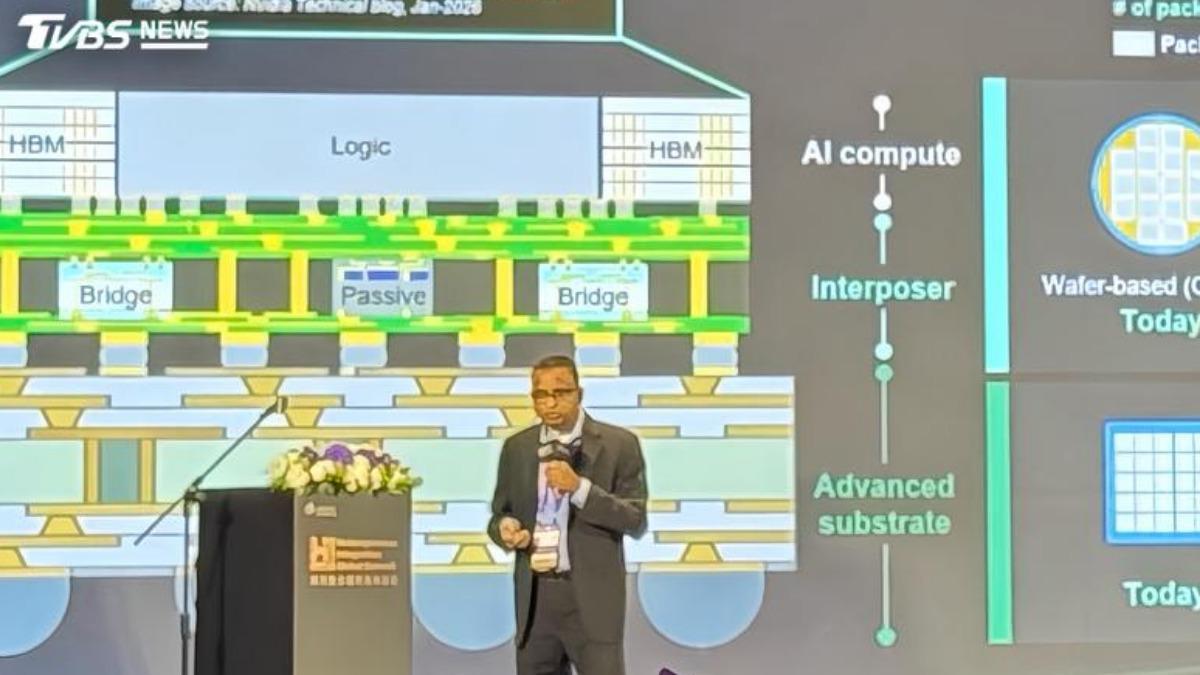
TAIPEI (TVBS News) — Panel-level packaging could offer higher area efficiency and economies of scale as AI chip packages grow larger, a Lam Research (科林研發) executive said Monday (Aug. 31). The technology addresses capacity and cost limits of conventional wafer-level packaging as demand for AI computing surges.
Thomas Ponnuswamy, product line head for Lam Research's Sabre 3D Platform, spoke at the FOPLP Innovation Forum (面板級扇出型封裝創新論壇) at SEMICON Taiwan (國際半導體展). Achieving wafer-level precision across much larger panels remains a key challenge, Ponnuswamy said. The forum is part of the HIGS Series events at the annual semiconductor trade show.
By 2030, a single AI package could reach an area equivalent to 14 reticles, Ponnuswamy projected. Such packages could integrate as many as 12 logic dies and 24 high-bandwidth memory stacks. The designs would adopt technologies including micro-bumps and hybrid bonding, driving demand for larger production formats.
The trend is exposing the limitations of circular wafers. A CoWoS package measuring 9.5 times the reticle size yields only about four packages per wafer. The geometry of round wafers creates significant material waste when producing large rectangular packages for AI applications.
Moving production to a 310-by-310-millimeter (12.2-by-12.2-inch) square panel could roughly double output compared with circular wafers. Larger panels measuring 510 by 515 millimeters (20.1 by 20.3 inches) or more could deliver further capacity gains. The square format eliminates edge waste inherent in round wafer production.
Panel-level packaging still faces several hurdles before reaching high-volume production. Manufacturers must control plating uniformity across large surfaces, manage edge and corner effects, and dynamically manage plating chemistry. Feed-forward calculations and real-time feedback systems can raise plating-solution recovery rates to more than 90%, Ponnuswamy said.
Warpage is another challenge as substrate sizes increase and the industry moves toward thinner glass substrates. Equipment makers are using machine learning to analyze equipment signals for predictive maintenance and improve tool matching across fabs. Automation can help reduce human error as panel-level packaging moves toward mass production. ◼